
The 555 timer IC.

This little but awesome 8 pin IC was invented in the year 1971 by Hanz camenzind. Personally i find it amazing to at least know a little history about anything, who knows, you might have to build up upon something someday.Read more about the history on wikepedia.
Anyway this is a short series on the 555 timer IC. This episode focuses more on the general and internal structure of the IC. Depending on where your interest lies you might not find it necessary to know what is really inside of the IC but trust me, it matters.

This green section is a voltage divider section and that’s where almost everything about the IC’s operation starts. The 3 resistors are of values 5 ohms each and they form a voltage divider connecting pin 8 which is VCC(voltage source) to pin 1 which is GND. This sets up 2 voltage levels, 2/3vcc and 1/3vcc at the 2 nodes. You can calculate this using the voltage divider rule. The first node from the top is the 2/3vcc and the second is the 1/3vcc. Read more about voltage division to understand this better.
If my eyes are not faulty, the yellow and red regions with the triangles are called comparators. Lets treat these two together since they are doing almost the same thing.
From the name, “comparator” you should know their jobs are to compare, and of course you don’t compare just one thing. You always compare something to a reference or standard. These comparators compare two voltage levels and give or deliver digital results of “1 or 0″ to their output depending on the comparison made.
A comparator has two analog inputs, a positive one and a negative one. In this diagram the negative input can be identified with that little blob or circle on the lower left of the camparator and the other is the positive. Depending on what you want the comparator to do, one of the two inputs are designated as “Vin” and ”Vref“.
The difference between the yellow and the red is their configuration.
The Yellow:
This one is a “non-inverting” comparator. A non-inventing comparator is a comparator that has the positive input to be its “Vin” and its negative input to be its “Vref”-refrence voltage. Such a comparator will ouput “logic 1” only and only if the Vin is greater than the Vref. So try think about it. Vref on this yellow one is already 2/3Vcc because of the node on the voltage divider it has been
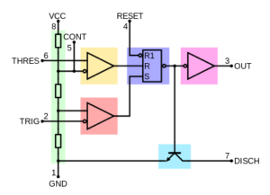
connected to. This means you’d have to supply a voltage greater than 2/3vcc to be able to output “logic 1” from its output. Anything lower will let the comparator bring out “logic 0”. Note that the output of the comparator is a digital output and the two inputs are analog.
“one day if someone asks you to mention any analog to digital converter system don’t forget to mention the comparator as one”
The Red:
This one is an inverting comparator. An inverting comparator has its negative input to be ‘Vin” and its positive input to be the “Vref”. Such a
comparator will output “logic 0” only and only if the “Vin” is lower than the “Vref”. This is opposite to what happens in the non-inverting comparator. Think a
bout it again. The Vref here is already connected to the 1/3Vcc node of the voltage divider, it means the Vin has to fall below 1/3Vcc before this comparator can have “logic 0” at its output.
So that is it about comparators and the role they play in the 555 timer.
The blue section is a called a flip-flop. Flip flops are electronic circuits that have two stable states and can be used to store data. They are the very basic storage devices used in digital systems and computers. There are about 4 types of flip-flop circuits which you can read more about, but for the purpose of understanding what is going on in this 555 timer, you should know that this is an SR flip-flop. SR flip flops are the most common and simplest you’ll probably come across in electronics.
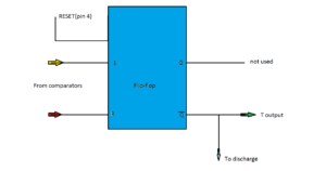
In the diagram above you can see it has 2 main inputs, the S and the R. It also has 2 output Q and Q’ but only the Q’ is used in the 555 timer.
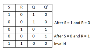
The table below shows the variations at the output Q’ when it receives the different inputs at S and R. Don’t forget that it is the output of the two comparators that have been connected to the S and R. So definately the input of this flip flip, S and R, will be “1s or 0s”
On the flip flop you can also see pin 4 which is the reset pin. It is used to override and reset the whole flip-flop. When you start using the 555 timer you will notice that pin 4 can be connected to ground to reset the whole action of the 555 timer when in operation.
This pink section is the output section. It is the circuit that drives whatever load you connect your 555 timer to. for example an LED. It is capable of sourcing up to about 200mA of current.
This output is a push-pull output. Push-pull here means it can both trigger your load by allowing current to come into it or it can trigger your load by allowing current to go out of it. In other words it can both drain and source.
And you can also see that it receives it input from the flip-flop. This means, it is the states(whether 1 or 0) which are stored in the flip-flip that will at the end of the day control the output driver and hence control the load you have.
I never knew this color was even called Cyan. This section is the discharge section. With the help of a transistor, it connects pin 7 which is the discharge pin to the ground. It is also activated by the same flip-flop circuit since the base of the transistor is connected to the flip-flop’s output.
Note that it is the charging and discharging rate of the capacitor in a 555 timer circuit that creates the timing property the 555 timer. This discharge pin helps the capacitor to drain down after it has charged fully so that the cycle can continue again.


Responses